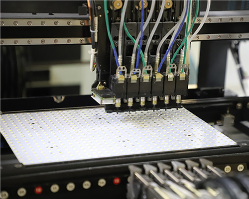
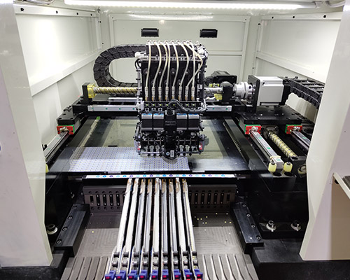
The Manufacturing Process
PCBs are the foundation of most modern electronic devices. They provide a platform for connecting electronic components and enabling them to communicate with each other. The manufacturing process of PCBs is complex and involves a series of precise steps to ensure functionality and reliability.Parts of the PCB
The PCB manufacturing process consists of complex processes which assures the better performance of the final product. The PCBs are divided into single, double or multilayer, the manufacturing process are same for first layer only. As there are various types of PCBs, some of them require more than 20 steps of manufacturing.
It is depending on the board types; the copper layer can be copper foil or entirely coated by copper. No matter how much copper is used, the purpose remains the same of carrying the electrical signals to and from the PCB.
How PCB are Made?
The manufacturing of Printed Circuit Board starts with,
Step-by-Step Guide to PCB Manufacturing
Step 1: Designing
The process begins with the creation of a digital blueprint of the PCB using specialized software like Extended Gerber (IX274X). This software allows designers to specify the number of copper layers, solder masks, and component placements.
Step 2: Design Verification
Once the design is complete, it undergoes a rigorous verification process to identify any errors or inconsistencies. This ensures the final product meets the desired specifications.
Step 3: PCB Design Printing
After design verification, the PCB design is transferred to a transparent film using a plotter printer. This film acts as a negative image of the PCB layout, with black ink representing copper traces and clear ink representing non-conductive areas.
Step 4: Copper Printing for Inner Layers
For multi-layer PCBs, separate films are created for each inner layer. The PCB laminate material is then bonded with copper foil, and a photosensitive resist is applied to the surface. Based on the film’s design, UV light is used to harden the resist in specific areas, protecting the desired copper traces during the etching process.
Step 5: Inner Layer Etching
The laminate panel is then etched with a chemical solution that removes the unprotected copper, leaving behind the designed copper traces.
Step 6: Layer Alignment and Inspection
Once the inner layers are etched, they are precisely aligned and inspected using an optical inspection machine to ensure proper alignment and identify any potential defects.
Step 7: PCB Layer Lamination:
All the PCB layers, including inner and outer layers, are laminated together using heat and pressure. A pre-preg resin layer bonds the individual layers, forming a solid and unified PCB structure.
Step 8: Drilling
Holes are drilled through the laminated PCB stack to create vias (connections between layers) and mounting points for electronic components.
Step 9: PCB Plating
The drilled holes and exposed copper surfaces are then plated with a thin layer of metal, typically copper or nickel, to ensure proper conductivity and protect the copper from corrosion.
Step 10: Outer Layer Imaging and Etching:
Similar to the inner layer process, a photoresist is applied to the outer layers, patterned with UV light based on the design film, and then etched to remove unwanted copper.
Step 11: Outer Layer AOI
Another automated optical inspection is performed on the outer layers to verify they meet design specifications and ensure proper functionality.
Step 12: Solder Mask Application:
A solder mask is applied to the PCB surface using a stencil and UV light. This mask protects desired copper areas from solder during component assembly while allowing solder to flow to designated connection points.
Step 13: Silkscreen Printing
Essential information such as component locations, logos, and warnings are printed onto the PCB surface using a silkscreen printing process.
Step 14: Finishing
A final surface finish, such as electroless nickel immersion gold (ENEPIG) or hot air solder leveling (HASL), is applied to the PCB. This coating protects the copper traces from oxidation and corrosion while facilitating component soldering.
Step 15: Reliability Testing
After completing all the above steps, the PCBs undergo a series of electrical tests to ensure proper functionality and identify any defects. These tests typically include continuity checks to verify connections and isolation tests to confirm there are no unwanted shorts between circuits.
Step 16: Profiling and Routing
Once the PCBs pass electrical testing, they are profiled using the Gerber files to determine their final size and shape. A computer-controlled machine then routes or scores the PCB panel, separating individual PCBs without damaging the edges.
Step 17: Final Inspection and Packaging
The separated PCBs undergo a final visual inspection to ensure they meet all the design specifications and quality standards. After passing inspection, the PCBs are carefully packaged to protect them from damage during transport and storage.
This concludes the step-by-step journey of PCB manufacturing. As you can see, it’s a complex and precise process that requires expertise and advanced technology. The quality and functionality of the final PCB depend on the accuracy and care taken at each stage of this multi-step process.